 Fraunhofer Institute for Process Engineering and Packaging IVV
Innovations in organic 3D electronics
RESEARCH PROJECT
FAQ - The most important questions and answers about conformable electronics
What restrictions are there for the development and manufacture of 3D electronic components?
An increasing number of everyday products have electronic functionalities such as sensors, lighting elements, displays, memories, and actuators. These are put on circuit boards and mounted into an assembly along with mechanical components such as operating and support elements.
This process is costly and time-consuming, puts considerable limitations on the design, and is prone to faults during the assembly. The best known alternative is 3D MID technology (3D Molded Interconnect Devices). This allows the printing and assembly of molded 3D components. However, this process is technically very complex and also very costly.
For this reason there is a need for favorable-cost technologies and processes for manufacturing the relevant products in large batch numbers.
How do we envisage the favorable-cost manufacture of printed 3D electronics?
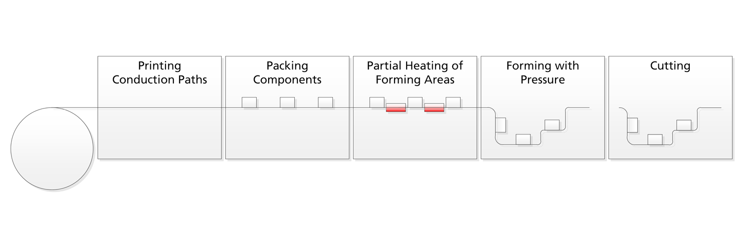
In order to keep the cost of manufacturing large batches of 3D electronic products, also known as 3D hybrid components, low for the mass marketplace, it is sensible to use conventional printing and assembly technologies used for circuit boards. This involves first of all printing and assembling the substrate (circuit board) in the flat state and then generating the 3D shape of the product via forming. This approach is known from the field of Conformable Electronics.
Favorable-cost, versatile, and rapid forming processes from the field of packaging technology are used for the printing and assembly. To meet the requirements for electronic products, innovative cera2heat® heating technology is being used in combination with a novel forming process. This allows precise control of the forming process and guarantees the required quality. In addition, design rules for printed 3D electronics are being drawn up. The manufacture of the products is being demonstrated using an R2R prototype plant.
What can this manufacturing process be used for?
The new manufacturing process and R2R plant enable the favorable-cost manufacture of innovative functional components in large batch numbers. The relevant components can be used for integrating sensors and actuators, for realizing greater design freedom, for reducing the manufacturing and assembly complexity, and for reducing the susceptibility to faults. In addition, the manufacture of moisture-resistant surfaces enables easy cleaning.
3D electronic components in R2R principle
Project partners
- Accomplast GmbH
- Adenso Industrial Services GmbH
- Adsphere GmbH
- Fraunhofer IZM
- OES Management GmbH
- TES Frontdesign GmbH